Several weeks back, I decided to re-explore the concept of hardware devices for storing GPG keys. The Yubikey Neo, 4, and 5 all have this functionality (with varying key-length options depending on the model), but these devices are not inexpensive ($40+, though Wired magazine has been running a deal for the past several months where you can get a Yubikey 4 with a 1-year subscription to the magazine for $5). In my search for inexpensive alternatives, I came across this post, where the author purchased very inexpensive ST-Link v2 clone devices and changed the firmware to an open-source hardware GPG implementation, called Gnuk. I have dabbled with hardware hacking more and more over the past few years, and I’m no stranger to flashing firmware (for example, I’ve been a long-time fan of DD-WRT and OpenWRT), so I thought this sounded like a really great project. The article was well written and had links to everything I needed to buy and install, so everything should be easy, right? Of course not, it never is, and that’s why I am writing this post rather than just letting you find the one I originally worked off of.
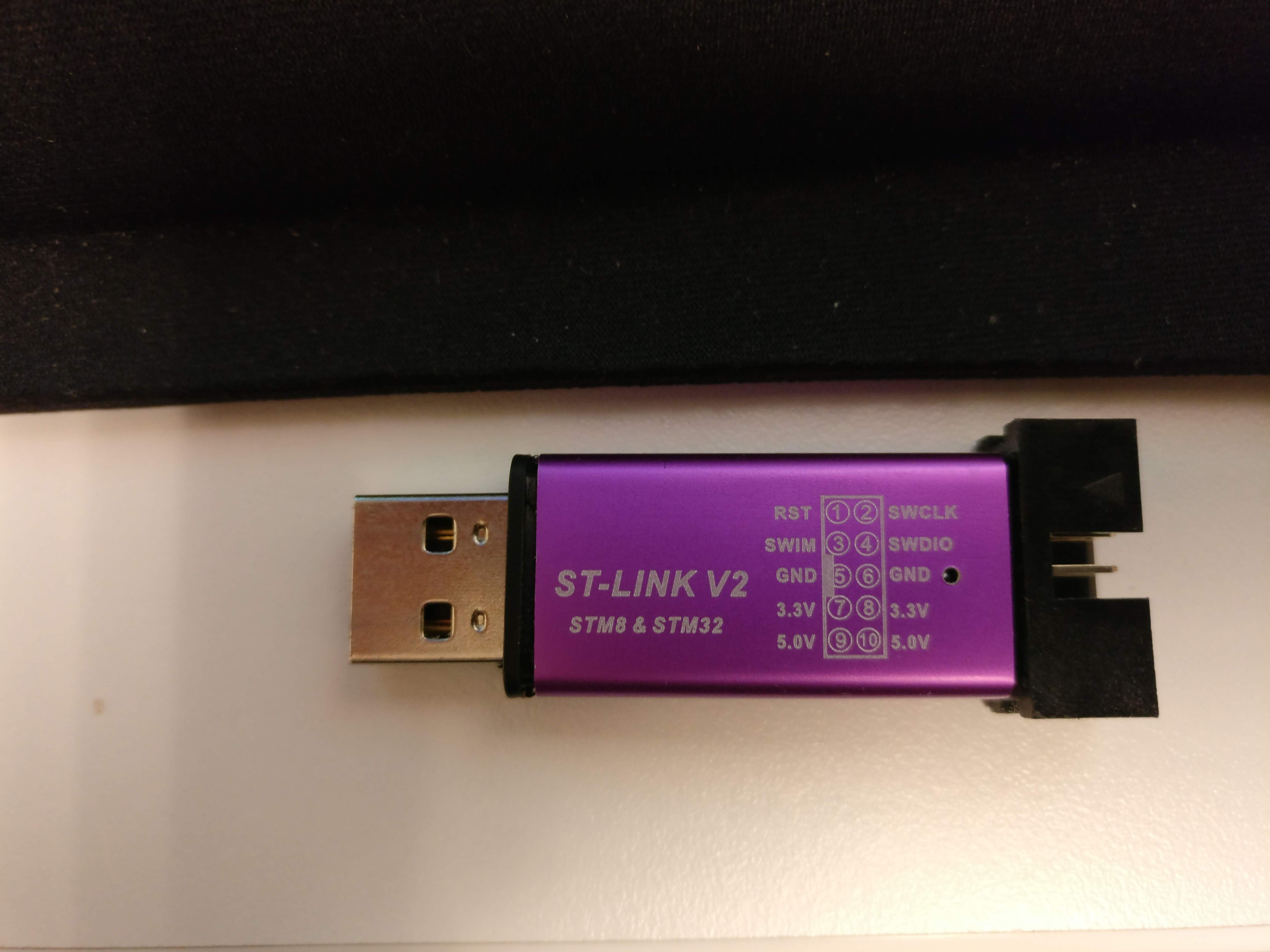
I was not initially familiar with the ST-Link v2, but I learned that it is a hardware tool used for interfacing with devices via SWD (Serial Wire Debug). SWD is a protocol found in ARM devices and uses fewer wires than JTAG. STMicroelectronics makes the official ST-Link v2 device, which I see via a Google search for between $10 – $25. AliExpress, however, has tons of sellers offering clone devices for approximately $2. These devices feature an STM32F103 microcontroller, which is compatible with the Gnuk firmware (or in other words, Gnuk offers this chip as a build target). I went searching on AliExpress and found myself the cheapest device I could (factoring in shipping) and bought 5 units. Why 5? I figured it’d be a cool little geek gift for some of my friends, potentially, but realistically I anticipated breaking at least one of them. Also, the nice thing about these devices is that you need an SWD programmer to re-flash the devices themselves, so you can actually use one of them to program the other ones. My order was estimated to arrive in 19-39 days, and I was pleasantly surprised when they arrived in around 15 days.
With the devices now on hand, I began by compiling the firmware. That was my first stumbling block. The repo where the project is stored had moved since the article I was referencing was published, so I needed to track that down. Eventually I found the repo, and cloned it onto my dev system (for reference, I was using Kali Linux, since that was the only Linux VM I had on my machine; any Debian-based variant should work fine with my instructions).
git clone https://salsa.debian.org/gnuk-team/gnuk/gnuk.git
cd gnuk/
git submodule update --init
cd src/
./configure --vidpid=234b:0000 --target=ST_DONGLE
mkdir build
make
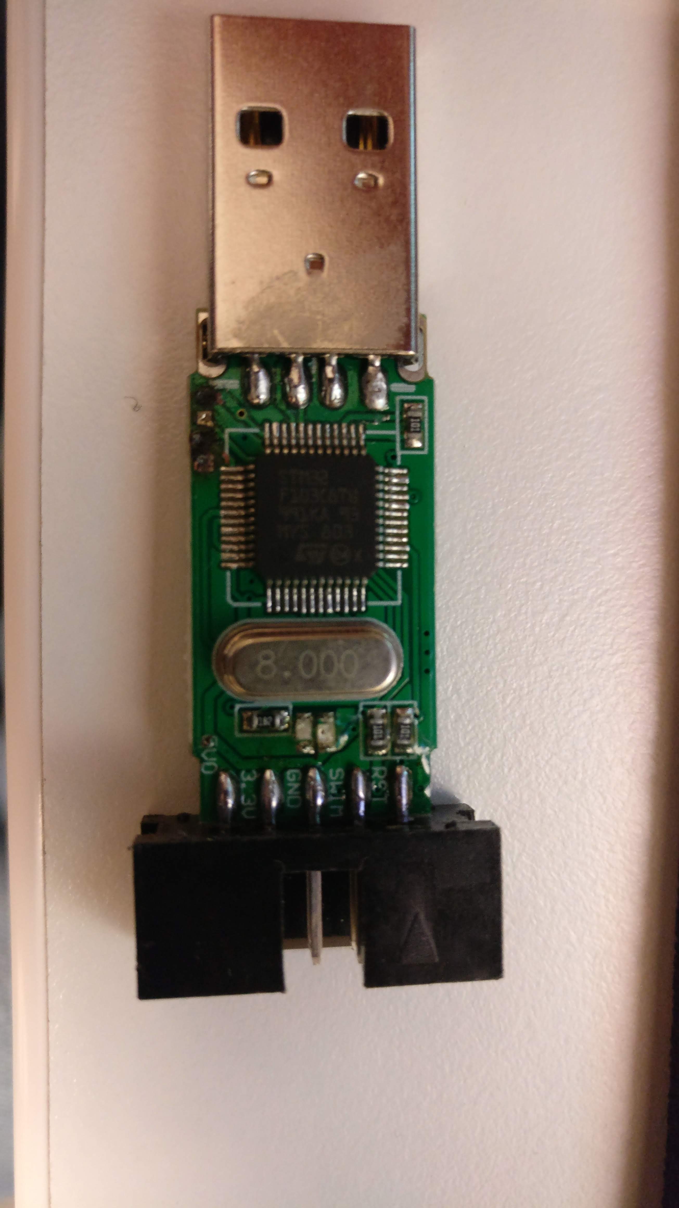
Once I built the firmware, I now needed to attach the device to my debugger and connect using OpenOCD. Initially, I tried using one of the ST-Link v2 devices I had purchased for programming another unit, but upon running into issues I instead tried using my Bus Pirate, which also supports SWD. However, I was unsuccessful in connecting to the device with either of these programmers. Multiple reference articles mentioned the debug layout as (starting from the spot closest to the USB port): SWDIO, GND, SWCLK, v3.3. Upon further inspection, I found that the units I had were physically different than those pictured in the article I referenced (and another that I found later). In the reference posts, the 4 debug points on the board were holes, going all the way through the board. On mine, however, they were just pads. The underside of the boards did not have any appearance of being connected to the topside, so I was not able to poke probes through the board for a good connection. That was the first hardware problem I encountered. I found that if I connected v3.3 and GND from the debugger to the target device (on the header pins, rather than the debug pads) I could power the device just the same as if I were connecting them to the debug pads, meaning I had fewer unwieldy connections to deal with. When that was connected, the device powered up, but I could not get any type of a data connection. For note, I was using clips to connect to the board, that way I could grab on to the pads since I couldn’t push anything through.
I decided that I would solder my probes to the board. So, I needed to buy a soldering iron, since I had no clue where mine was (it’d been years). I decided on a kit that contained a multimeter included, that way I could test the voltage levels coming from the board. I want to approach this slightly less blindly than I had thus far. Once that kit arrived, I attempted to solder wires to the 2 data pads on the board (pads 1 and 3, if counting from 1, with 1 being closest to the USB port). I *finally* was able to get it soldered (this stuff is really small!), but I still could not get it to connect to the ST-Link or Bus Pirate. Also, I burned the crap out of some of the debug points in the process (some out of error, some out of frustration). I then bust out the multimeter and started probing the board. What I found was that the points on the board were not only physically different than the reference article boards, but they were actually arranged differently too. I found that point 1 was v3.3, and point 4 was GND. Upon connecting power to point 1 and ground to point 4, the LED lit up just as it had when connecting to the header pins, so I knew at least those points were correct. Point 2 and 3 had to be SWDIO and SWCLK, right? Thankfully there are only 2 combinations I needed to test to identify which point was which. Guess which combination worked? Neither!
At this point I was at a loss. I thought I had done everything correctly from a trouble-shooting standpoint, but I could not explain why those two points on the board would not give me debug access. In my frustration, I ended up buying 2 more sets of 5 boards each from AliExpress, from 2 different sellers, each with multiple pictures of the board showing that they had debug holes rather than pads. That was 2 days ago, and now I needed to wait another 15-30 days for them to arrive. So much for this being an easy, fun project… For reference, these are the two ones that I bought that I’m still waiting to arrive that *should* be much easier to make work: https://www.aliexpress.com/item/ST-Link-V2-Programming-Unit-mini-STM8-STM32-Emulator-Downloader-M89-New/32631496848.html?spm=a2g0s.9042311.0.0.15ff4c4djHAJY3, https://www.aliexpress.com/item/1Set-ST-LINK-Stlink-ST-Link-V2-Mini-STM8-STM32-Simulator-Download-Programmer-Programming-With-Cover/32887597480.html?spm=a2g0s.9042311.0.0.15ff4c4djHAJY3. This is the bad one (stay away from it!): https://www.aliexpress.com/item/1PCS-ST-LINK-Stlink-ST-Link-V2-Mini-STM8-STM32-Simulator-Download-Programmer-Programming-With-Cover/32792925130.html?spm=a2g0s.9042311.0.0.15ff4c4djHAJY3
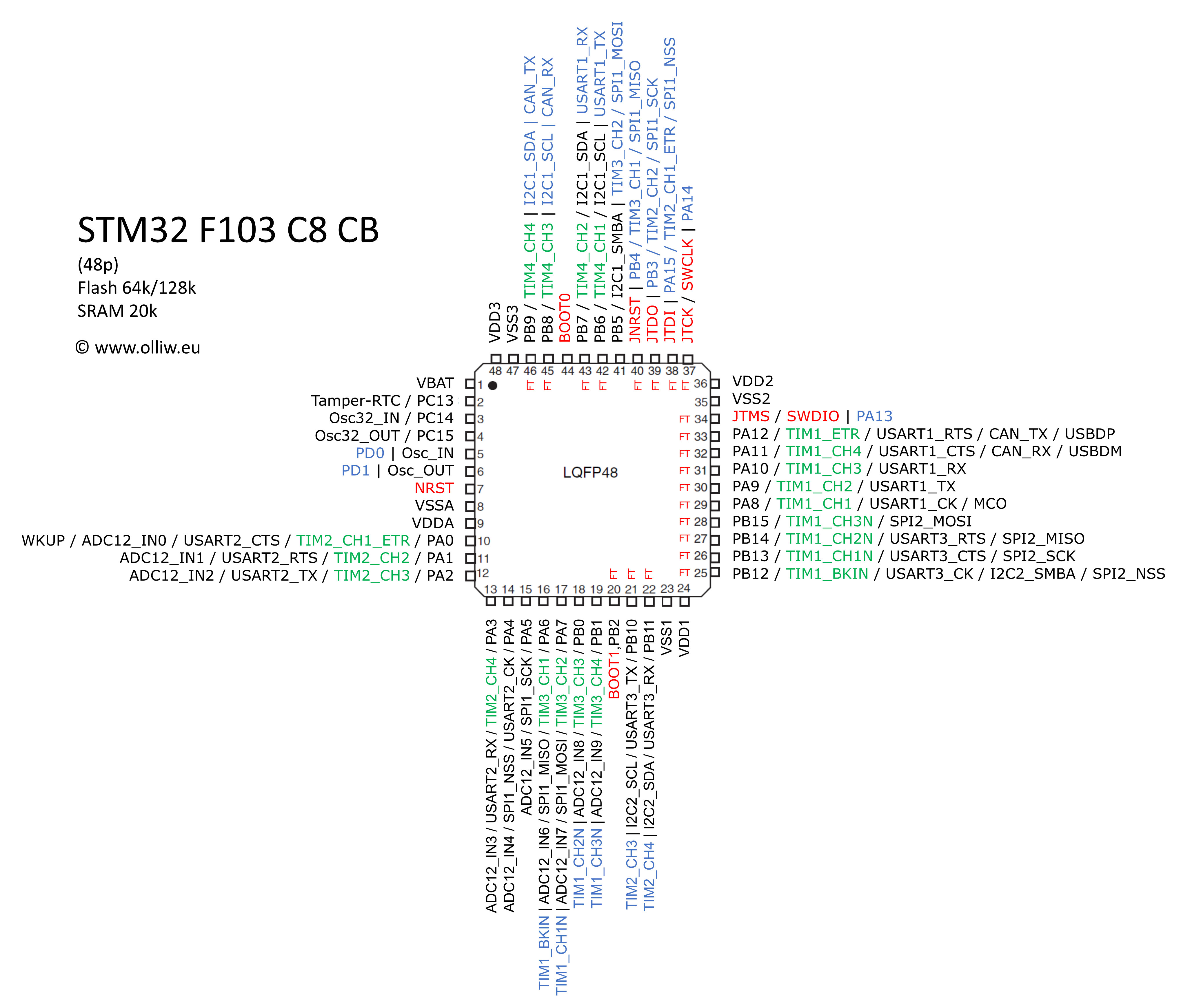
I’m curious and impatient, though. So yesterday I decided to take one more stab at this. I had no idea what debug points 2 and 3 were on that board and why they would not give me SWD access to the chip. However, I knew what the chip itself was (due to the imprint on it that said “STM32F103”), so I thought that could help. I Googled the pinout of the chip and identified the SWDIO and SWCLK pins. In the image below, you can see that pin 34 corresponds to SWDIO and pin 37 is SWCLK.
So, now that I knew which pins on the actual chip were needed for debugging, I attempted to connect my clips to the pins. This was about as difficult at first as I expected, as these pins are super small. I couldn’t get pin 34 connected by itself, though I appeared to be able to connect pin 37 (since it was at the end of a row, and as such easer to grab). Eventually though, I decided to give up on precision and just to attempt to make contact with the pins by grabbing each one needed and a few around it. That was much easier than attaching just to the single needed pins. Note: I don’t know if this would work on similar or different chips, and I suppose it could potentially cause damage, so proceed with caution.
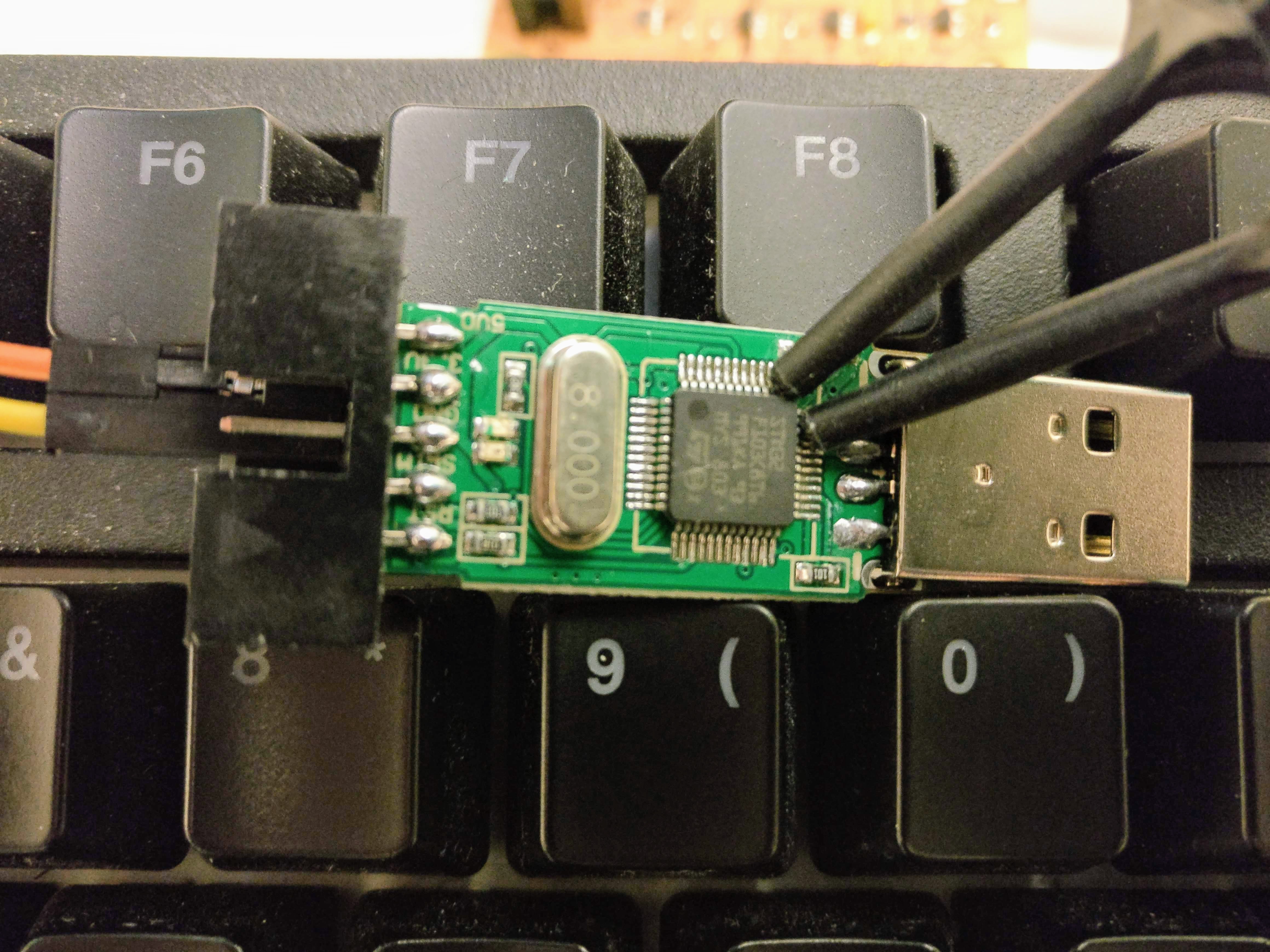
I fired up OpenOCD using my Bus Pirate, and was finally able to connect! Hallelujah! I was able to execute the needed commands to unlock the device, reset it, and erase the flash. However, I was not able to write my firmware file. Maybe I was just too impatient, but I literally gave this thing 20+ minutes to write a 128KB file, and it just wouldn’t. From the other posts I read, it appeared from the output of OpenOCD that it should only take a matter of seconds to write the file. Frustrated again, I decided to try to use one of the devices I bought to act as the debugger, too. I used the OpenOCD configuration below to connect.
Note: if you don’t have OpenOCD already, you can install it by typing:
sudo apt install openocd
OpenOCD config for ST-Link v2 (called openocd.cfg moving forward):
telnet_port 4444
source [find interface/stlink-v2.cfg]
source [find target/stm32f1x.cfg]
set WORKAREASIZE 0x10000
To connect, run the command:
openocd -f openocd.cfg
You should see the a message about connecting to the device, and it should not exit within a few seconds. After that, you need to open a new terminal and connect to OpenOCD using Telnet:
telnet localhost 4444
Once connected via Telnet, you need to unlock the device, reset it, erase memory (for good measure), write the Gnuk binary, lock the device, and then reset it once more:
reset halt
stm32f1x unlock 0
reset halt
stm32f1x mass_erase 0
flash write_bank 0 /root/src/build/gnuk.bin 0
stm32f1x lock 0
reset halt
After that, once you connect the device to the USB port of your machine it should be detected as a GPG card! You can confirm by running the command:
gpg --card-status
References:
https://nx3d.org/gnuk-st-link-v2/
https://blog.danman.eu/2-usb-crypto-token-for-use-with-gpg-and-ssh/ https://www.earth.li/~noodles/blog/2015/08/program-fst01-with-buspirate.html
hello,
this is a fun technical experiment, but it would need some tricks to be at least minimally secure:
-program security fuses to forbid jtag/swd/code readout.
-make sure the ST system bootloaders cannot be used to dump the flash. Devices have multiple bootloaders: USB DFU but also SPI, UART and CAN.
-make sure the bootloader cannot be used to upload a malicious firmware that would be able to dump your keys. Some bootloaders forget to mass erase the full user programmable zone, and leave some sensitive material accessible to a separately loaded firmware image. No need to sign the firmware, it is enough to ensure that your private keys are destroyed if the firmware is updated.
yet, the stm32f103 is vulnerable to code dumping even with these protections, so
-desolder, and CUT all useless pins.
-mill the package to physically remove the lead frames in the package, all the way to the bonding wires
-remove the 10-pin SWD connector
-fill the aluminium can with two-component epoxy, or better, metal loaded JB-weld after a thin insulating coating.
You’re correct, this by itself definitely isn’t safe for many of the reasons you listed. Great suggestions for improving security, however my recommendation would be to just avoid this altogether and go with a purpose-built product if you are concerned with the security of your device.